APhO 2019, Теория — Задача 1. RF reflectometry for spin readout for silicon quantum computing
Asian Physics Olympiad Adelaide 2019 — Theory Q1: RF reflectometry for spin readout for silicon quantum computing
Условие
Introduction
Developing the idea of quantum computing into a practical technology is one of the largest outstanding challenges in science and technology. A promising path is to manipulate individual electrons in silicon transistors by time-dependent electromagnetic fields.
In this question, we investigate the use of radio frequency (RF) reflectometry and single-electron transistors to read out the state of quantum bits in silicon-based quantum computer prototypes.
Part A and Part B discuss radio wave transmission through cables and transmission lines, part C is devoted to conditions for wave reflection, part D introduces the single-electron transistor, and parts E and F introduce and ask you to optimise the method of reflectometry.
Part A: Lumped element model of a co-axial transmission line (2.0 points)
When modelling DC or low frequency signals, one often assumes that a voltage pulse travels instantaneously throughout the circuit. This assumption is valid when the wavelength of such signals is much longer than the size of the circuit, however when working with radio frequency signals, the dynamics are more complex, and we need to account for the intrinsic capacitance and inductance of our cables in our model. We model a co-axial transmission line which acts as a waveguide as described below, ignoring the small resistance of the copper and the small conductance through the dielectric. Throughout the problem, we consider the large-wavelength limit of electromagnetic waves in the co-axial cable such that electric and magnetic fields are perpendicular to the axis of the cable everywhere (the so-called transverse electromagnetic mode).
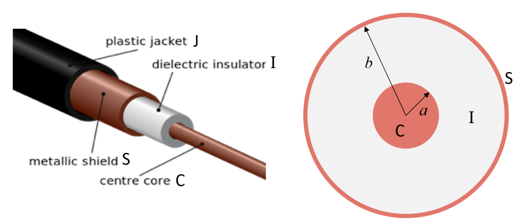
Consider a co-axial cable consisting of a copper inner core of negligible resistance, negligible magnetic permeability and radius , covered by an outer co-axial copper shield with inner radius . A dielectric of dimensionless relative permittivity and dimensionless relative permeability separates the layers. When electromagnetic signals propagate through the co-axial cable, they are confined between the inner core and outer shielding.
A.1 At what speed do electromagnetic waves propagate in the co-axial cable? [0,2 т.]
A.2 If there is a charge on a length of the inner core of the co-axial cable, and the outer shield is grounded, find the electric field in the region between the inner core and the shield. [0,2 т.]
A.3 Find the capacitance per unit length, , of the co-axial cable. You may wish to consider a length of the cable. [0,3 т.]
A.4 Find the inductance per unit length, , of the cable. [0,3 т.]
A lumped element model of the cable is constructed by considering the inductance and capacitance of short sections of the cable. The inductance is assumed to be a property of the inner core, and the capacitance links the core with the shielding. A diagram of the lumped element model is shown below.
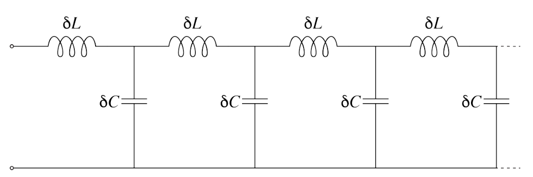
A.5 i. Show that the impedance of a semi-infinite length of cable is .
ii. Find if the cable has impedance and is made using a dielectric material with and . [1 т.]
Part B: Hypothetical transmission line with return along a grounded plane (1.0 points)
An alternative hypothetical transmission line is shown in the diagram below. The input signal is sent through a very thin conductor of radius , which is a distance from a highly conductive grounded plane. The material surrounding the conductor has dimensionless relative permittivity and dimensionless relative permeability . The return current flows along the grounded plane.
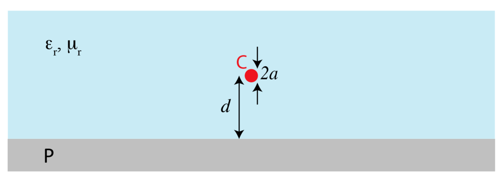
B.1 Find an expression for the characteristic impedance of this hypothetical transmission line. [1 т.]
Part C: Basics of RF reflectometry (1.2 points)
An electromagnetic wave can propagate in a transmission line in two opposite directions. For each direction of propagation, the characteristic impedance can be used to relate the voltage and current amplitudes as in the Ohm's law, .
Consider an interface between two transmission lines, with characteristic impedances and . A schematic diagram of the circuit is shown below.
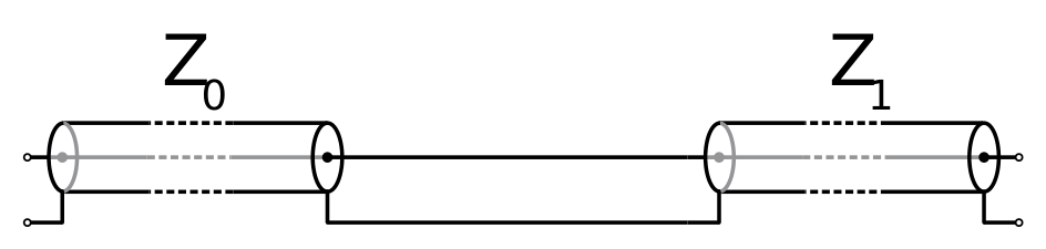
When a signal sent into the transmission line with impedance reaches the interface it is partially transmitted into the second transmission line, resulting in a signal in that line which propagates forward. Some of the signal may also be reflected, resulting in a backward propagating signal in the initial transmission line .
C.1 Find the reflectance of the interface . [1 т.]
C.2 State the condition(s) for the signal to have gained a phase change on reflection. [0,2 т.]
Part D: The single electron transistor (3.3 points)
A single electron transistor (SET) consists of a quantum dot, which is a small isolated conductor where electrons can be localised, and of several electrodes in its vicinity. The gate electrode couples capacitatively to the quantum dot, while the two other electrodes --- the source and the drain --- are connected via tunnel junctions, through which electrons can tunnel due to quantum mechanics. A simplified circuit diagram for an SET is shown in the figure.
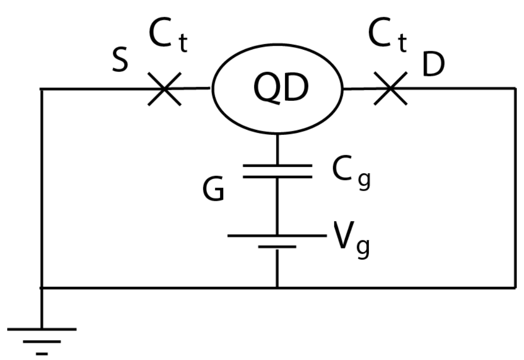
The capacitance of the gate is and the capacitance of the tunnel junctions is . Consider to be the total capacitance of the quantum dot. In this part of the problem, the source and the drain are held at zero potential, and the voltage on the gate electrode is fixed at .
D.1 Consider a state of the SET in which the quantum dot contains electrons.
i. Find the electrical potential on the QD.
ii. Find the amount of energy that is necessary to bring an additional electron from the source or the drain onto the QD. [1,5 т.]
If then electrons will spontaneously tunnel into the quantum dot until such a number is reached that . The equilibrium number of electrons and the corresponding addition energy can be controlled by choosing the appropriate voltage .
D.2 Find an expression for the maximal possible value of the equilibrium addition energy that can be achieved by tuning the gate voltage of the SET. [0,5 т.]
If then tunnelling of electrons does not require extra energy and SET is in a highly conductive ON state. If , then the conductance of the SET is reduced (high-resistance OFF).
For the number of electrons on the quantum dot to remain well-defined, certain conditions need to be satisfied. Firstly, if electrons in the source or drain have thermal energies sufficient to move spontaneously onto the quantum dot, the contrast between the ON and OFF states will disappear.
D.3 Find a condition on the temperature of the electrons so that electrons cannot move onto the quantum dot by thermal excitation. [0,5 т.]
Secondly, tunnelling of electrons onto or off the dot limits the lifetime of their energy states. This tunnelling can be modelled using an effective resistance of the tunnel junction with the characteristic tunnelling time equal to the characteristic time for charging or discharging the quantum dot through the junction.
D.4 i. Estimate the tunnelling time for a quantum dot in terms of capacitance and effective resistance of the tunnel junction.
ii. Find a condition on the effective resistance so that the electrons in the quantum dot retain sufficiently well-defined energy for the ON and OFF states to remain distinct. [0,8 т.]
Part E: RF reflectometry to read out SET state (1.0 points)
The state of the SET is sensitive to electrical potentials created by nearby elements of the quantum circuit (such as quantum bits), and distinguishing between ON and OFF states provides a way to read out the information produced by the quantum computer. The SET in the ON state can be modelled by a resistance while in the OFF state we can assume the SET to be a complete insulator (neglecting any capacitative connection between the source and the drain via the SET). While it is possible to determine the state of the SET by measuring the response to an input signal through the source, it is faster to do so using RF reflectometry to measure both the amplitude and phase of the reflected signal, i.e. determined the reflectance .
The change in reflectance due to switching of an SET between ON and OFF states is
where and are the reflectances in two different states.
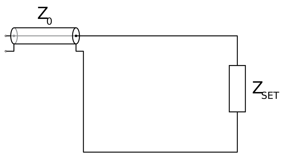
E.1 Find the change in reflectance between the conductive and insulating states for a typical SET connected to a co-axial cable with impedance of . [0,2 т.]
In order to increase the change in reflectance, and hence the sensitivity of the RF reflectometry, the circuit is modified by inclusion of an inductor. The intrinsic capacitance due to the device geometry is also taken into account. The RF reflectometry is conducted using a signal of angular frequency .
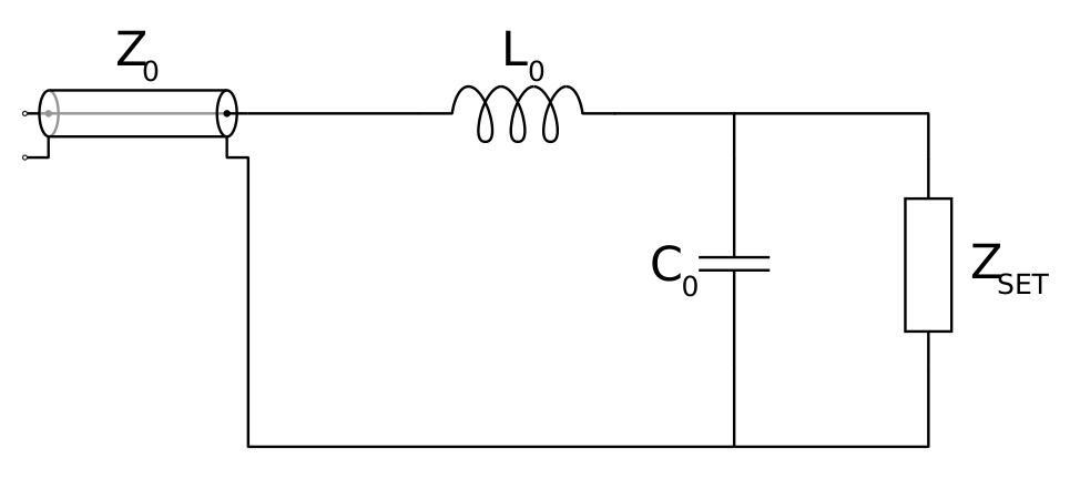
E.2 Estimate the value of the inductance that can result in the change in reflection on the order of one. Calculate your estimate for numerically for and compute the corresponding . [0,8 т.]
Part F: Charge sensing with a single lead quantum dot (1.5 points)
For a scalable quantum computing architecture, the number of wires reaching each individual quantum bit need to be minimized. A promising alternative to an SET for charge sensing in silicon quantum computing is a Single Lead Quantum Dot (SLQD). In many ways it is similar to an SET, but does not have the source and drain leads. The gate is the only electrode, through which the electron energy states of the quantum dot are controlled and also through which RF reflectometry is conducted.
Like an SET, a SLQD has an OFF in which the SLQD behaves as a total insulator. In contrast to an SET, the ON state of the SLQD is capacitive, with capacitance . In order to maximize the difference in reflectance of the SLQD, the following circuit is constructed. The parasitic capacitance is fixed by circuit geometry, but the value of and the operating frequency can be changed to optimize the performance. The characteristic impedance of the transmission line is .
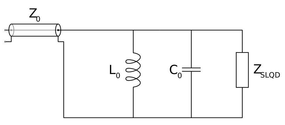
F.1 Suggest and that allow for given and . [1 т.]
Optimal values of are relatively large and not always technically feasible. Hence, other types of circuit elements may be needed to improve sensitivity of the reflectometry readout circuit.
F.2 Assume that (and hence ) is fixed. Draw a circuit diagram showing where to place an additional element in the SLQD readout circuit and specify the parameter(s) of this element such that can still be achieved without requiring a large inductance. [0,5 т.]
Отговори
A.1
A.2
A.3
A.4
A.5
Official: .
B.1
C.1
C.2
D.1
D.2
D.3
D.4
E.1
E.2
F.1
F.2
Official: an additional capacitance in series with the rest of the circuit, operated at .
Решение
Theory Q1: Solutions
RF Reflectometry
Version 1.32.
A. LUMPED ELEMENT MODEL OF A CO-AXIAL TRANSMISSION LINE
A.1 The speed of wave propagation in free space () is . The speed in the dielectric & diamagnetic medium is
A.2 Gauss law for the flux through a cylindrical surface with radius co-axial with the the core, :
A.3 The capacitance
where the potential of the core with respect to the shield is
A.4 The magnetic flux through a rectangular contour parallel to the axis equal inductance times the current:
Biot-Savart law gives
A.5 i. Adding length of the cable should not change its impedance. Hence the impedance of the following circuit must be equal to :
(here engineering notation for is used.) and for , hence
ii.
For , and this gives .
B. HYPOTHETICAL TRANSMISSION LINE WITH RETURN ALONG A GROUNDED PLANE
B.1 The high-conductance ground plate can be replaced by an image of the wire with opposite direction of the current at distance from the real wire. The magnetic fields from the real and the imaginary wires add up and need to be integrated to get the magnetic flux between the wire and the plate:
The potential difference between the wire and the plate can be obtained similarly by integrating the combined field for the wire and its image:
Hence the characteristic impedance of the wire-plate system is
C. BASICS OF RF REFLECTOMETRY
C.1 At the interface, values of the voltage on both transmission lines have to coincide:
The current has to be conserved at the interface, however, the incident and the reflected waves carry the current in opposite directions:
It is clear from the equation above that if – impedance mismatch has to cause reflection. Solving the voltage and the current equations for gives
C.2 A -shift implies opposite signs of and and hence requires . This implies .
D. THE SINGLE ELECTRON TRANSISTOR
D.1 i. Since any capacitance beyond is neglected in our model, the quantum dot can be thought as a capacitor plate with the gate being the other plate of the same capacitor with capacitance . The fixed number of electrons trapped on the quantum dot sets a fixed-charge () boundary condition for the capacitor on the QD, while the gate side is kept at a constant potential . (We denote the elementary charge by ). The implies that an excess charge of opposite sign, will accumulate on the gate, to keep electric field confined between the QD and the gate. The potential jump across the capacitor from the gate to the QD will be equal to the capacitor . Hence the potential on the QD is
ii. Bringing an infinitesimal charge from potential 0 to potential requires energy , and the dependence of potential on the accumulated charge is linear. For the single-electron transfer, the additional charge of the electron, , changes the potential from to . Hence the work necessary to accumulate an extra on the QD is the integral of
Alternatively, can be obtained from energy conservation, by computing the change of the energy of the capacitor the dork the work done against the electromotive force of the battery (=−“work done by the battery’) for a charge to be brought from the ground potential via the battery to the gate-side plate of the capacitor:
Note that without approximation, the answer is (not required to receive full marks).
D.2 is a minimal integer for which . Consider the marginal case of which is achieved at some ,
If would go slightly larger than , then would go negative and then minimal that makes a positive would jump from to . Hence . This gives
D.3 In a metal, only electrons in an energy range around the Fermi level take part in the thermal motion. (Here is the Boltzmann constant.) Typical energy of these electrons is per particle and it may not exceed characteristic single-electron addition energy , .
D.4 i.
ii. Quantum uncertainty of energy (life-time broadening) must be less than the energy difference between the states with and electrons,
E. RF REFLECTOMETRY TO READ OUT SET STATE
E.1
E.2 Large change in reflectance requires the impedance of the circuit to switch between to as the SET between ON () and OFF ().
In the OFF state of the SET, the circuit is an dissipationless LC contour with resonance frequency and its impedance is 0. If we choose
then the impedance of the .
Since (the total impedance of the circuit) in the OFF state of the SET equals to 0, the reflectance i . As we switch to the ON state with , the change in reflectance will be large if in this ON state is on the order of or larger, which is indeed the case.
For the ON state and
For , and , we have , , , and .
F. CHARGE SENSING WITH A SINGLE LEAD QUANTUM DOT
F.1 The SLQD readout circuit contains only reactive elements, so will always be one. The OFF state of the SLQD corresponds to an inductor and a capacitor connected in parallel. We again choose
so that is the OFF state is infinite and .
The ON state corresponds to and at is just the impedance of the SLQD
For the complex phase of to be significantly different from zero, we need since is purely imaginary. Hence
F.2 If is fixed, we can still operate the circuit at the frequency
that gives . However, we need to deduce a way to increase even if is not sufficient. One of the ways to do that is to add an additional capacitance is series with rest of the circuit. This will give (at )
We can satisfy the condition (and hence and ) with