Thermal oxidation is the process of creating a very thin (tens/hundreds of nanometres) film of silicon dioxide SiO2 on the surface of silicon Si at high temperatures. This technology is an essential part of the manufacturing process of integrated circuits and MOSFETs (metal-oxide-semiconductor), which form the basis of modern electronics. If you place silicon Si in an aerobic environment, the oxidation process of Si+O2→SiO2 will begin. For the description of crystalline silicon and flat oxide films of sufficient thickness (starting from ten nanometres), the Dill-Grove model (1965) does well, but a detailed description of the growth mechanism in other conditions is still an unsolved scientific problem.
Silicon is opaque to visible light, while its dioxide is transparent. These optical properties, combined with the fact that the dioxide film has a thickness of tens of nanometres, create ideal conditions for very precise optical control of the thickness of the SiO2 layer.
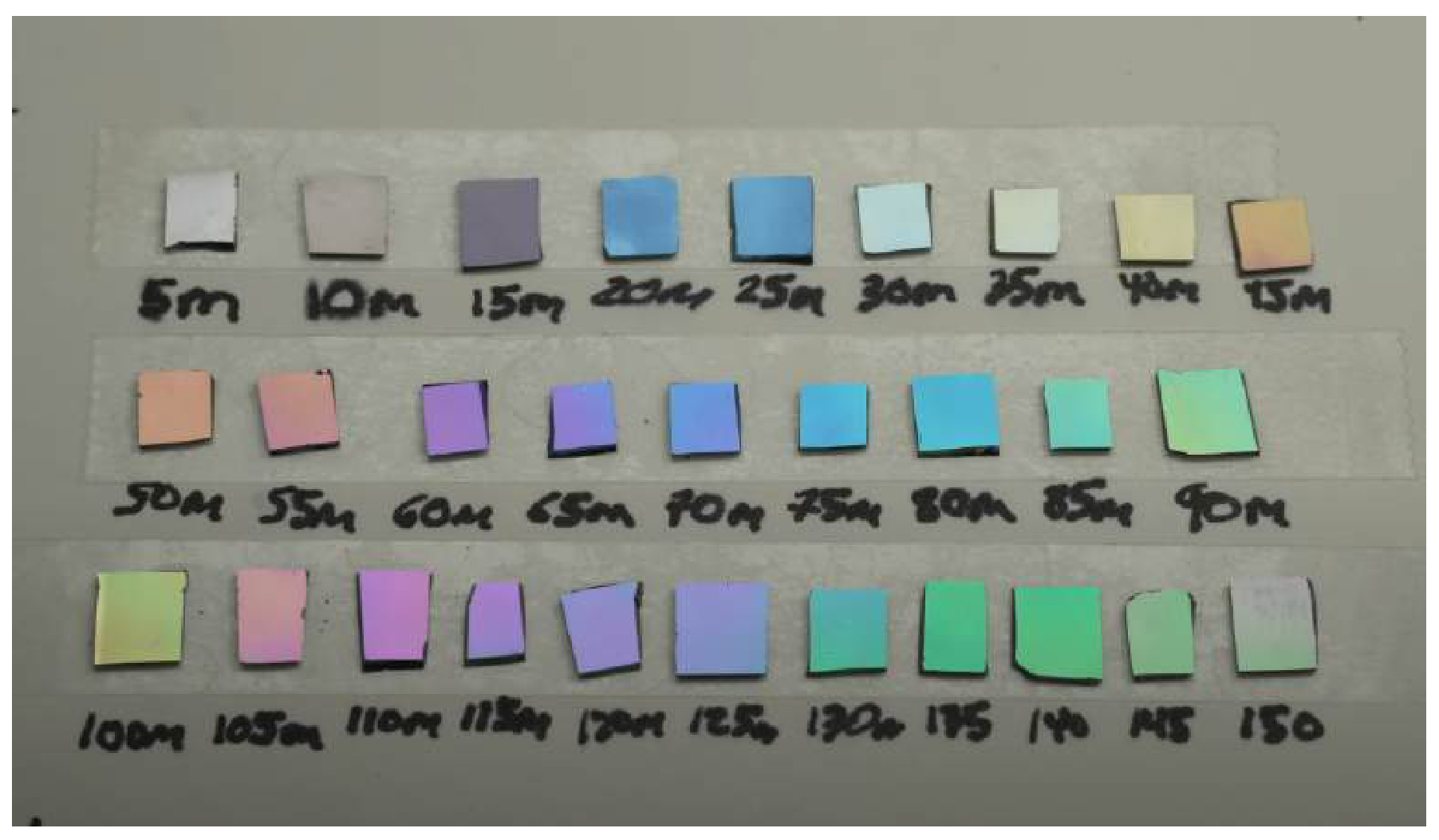
The change in the visible color of the silicon substrate at different oxidation times. ”Growing Colorful Oxide Layers on Silicon” by ProjectsInFlight on YouTube.
We will investigate the film growth by using ellipsometry, a powerful technique for studying the optical properties of thin films. It is based on a comparison of the amplitude coefficients of reflection of s-polarized and p-polarized waves (from the German ”senkrecht” – perpendicular, ”parallel” – parallel) from the surface of the film. The measurement results are represented by ellipsometric angles Ψ, Δ:
rsrp=tanΨ⋅eiΔ,
where the value of Ψ corresponds to the ratio of amplitudes upon reflection of p- and s-polarized waves, and the value of Δ corresponds to the phase difference between them.
Ellipsometry measures precisely the relative difference between waves (ratio of amplitudes and phase difference) with different polarizations, so it is very resistant to various fluctuations in the power of the radiation source and the sensitivity of the receiver. Ellipsometry also makes it possible to measure the characteristics of a sample without direct mechanical contact with it, which allows measurements to be carried out in real time and in situ (from lat. – ”on the spot”, directly).
During the entire task, the wavelength of the incident wave is marked as λ. In the optical range, substances do not have significant magnetic qualities, therefore, all materials under consideration have μ=1.
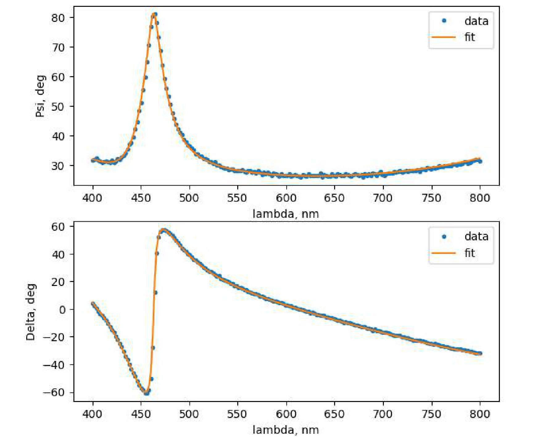
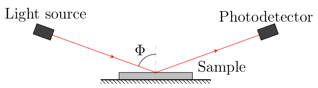
Example of an ellipsometric spectrum Ψ,ΔOptical scheme of the ellipsometer: a light source, a Photodetector, and a test sample.
Attention! Place the files you want to attach to the report in the “report” folder.
Attention! It is enough to make only A7 to moving on to part B.
Part A. Theoretical principles of ellipsometry
Maxwell’s equations in a non-magnetic dielectric have the form
divD=0rotE=−∂t∂B
divB=0rotB=μ0∂t∂D
For a dielectric:
D=ε0εE
It follows from these equations that the normal components of the vectors D and B as well as the components of the vectors E and B directed along the surface do not change at the dielectric-dielectric boundary.
In a plane wave the wave vector, the electric field vector and the magnetic field vector k, E and B are pairwise perpendicular and right-handed orientated. Also hold the following relations:
B=ω1[k×E],∣k∣=εω/c
where ω is the frequency of the wave. The speed of light c=1/ε0μ0. As a part of this task, we will consider the interaction of a plane wave with layered structures and develop a general approach for the theoretical description of such a system. Let a film with a thickness d be made of a material with dielectric permittivity ε2 be located between two semi-infinite dielectrics with dielectric permittivity ε1 and ε3 respectively.
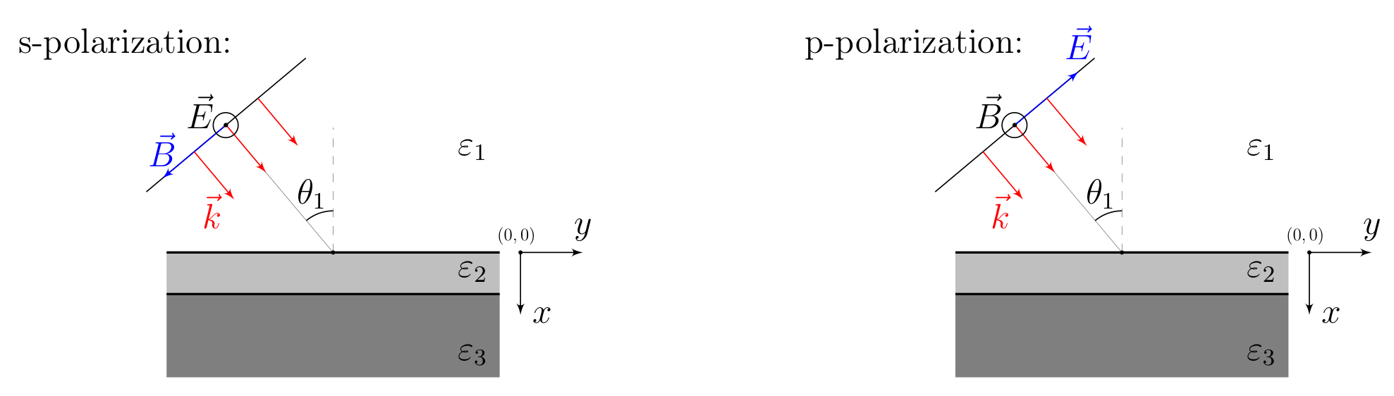
When a incident wave falls on the film, a reflected wave occurs in the medium ε1, a passing wave in the medium ε3 and a superposition of waves going in different directions in the medium ε2. In s-polarization, the direction of the electric field is fixed, so we can proceed to consider scalar complex amplitudes:
In p-polarization, the direction of the magnetic field is fixed, so it is easier to proceed to the consideration of scalar complex amplitudes of the magnetic field:
The incidence of the s-polarized and p-polarized wave on the film
A1 Show that k1y=k2y=k3y.
A2 Find expressions for k1x, k2x and k3x in terms of ω, c, θ1, ε1, ε2, ε3.
A3 For a wave with s-polarization (the electric field is directed along the surface), from the boundary conditions for the tangential components of the fields, obtain a system of linear equations for the coefficients r, A, b and t.
A4 Find the reflection coefficient. Bring the answer to the form:
rs=AB+e2ik2xdA+Be2ik2xd.
Express the real numbers A, B in terms of k1x, k2x and k3x.
For convenience, use the variables κix=εikix for i∈[1,3].
A5 For a wave with p-polarization (the magnetic field is directed along the surface), from the boundary conditions for the tangential components of the fields, obtain a system of linear equations for the coefficients r, A, b and t.
A6 Find the reflection coefficient. Bring the answer to the form:
rp=AB+e2ik2xdA+Be2ik2xd.
Express the real numbers A, B in terms of k1x, k2x and k3x.
We will perform preliminary calculations of the approximate shape of the ellipsometric spectrum of a thin layer of silicon dioxide on a silicon substrate. Until the end of Part A, we will neglect the optical dispersion, and assume εAir=1.00, εSi=17.2−0.430i, εSiO2=2.13. Note that silicon has an imaginary part of the dielectric constant responsible for absorption, due to which it is opaque. The use of complex permittivity does not change obtained expressions, if the trigonometric functions of the complex parameter are considered.
With the help of the A.py program, you can plot Ψ and Δ for different angles of incidence θ1 and thicknesses d. At the input, the program receives the name Name of the series, the angle of incidence θ1 from the air (in degrees) and the thickness d of the dioxide film in the form of a table written in the file A_in.txt .
There is an example of filling in a table in a file A_in.txt:
Name
θ1,∘
d,nm
ex1
50
40
ex2
30
100
⋮
⋮
⋮
The input data is limited to 20∘≤θ1≤80∘, d≤250 nm. The name of the experiment should not contain spaces and tabs. The separator between the integer and fractional parts of numbers is a dot. The separator between the columns is a tab.
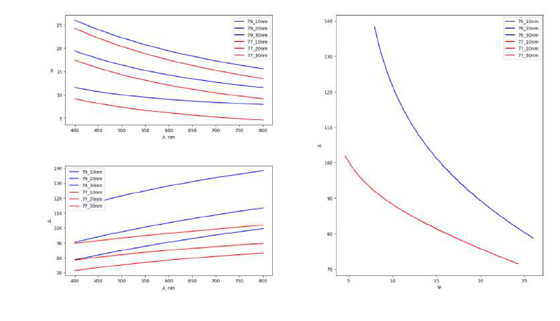
A7 Using the program A.py plot the dependence of Ψ and Δ on λ at different angles of incidence θ1 and thicknesses d. Conduct a quantitative study and determine at which angle of incidence θopt the ellipsometric angle Ψ is most sensitive (the highest value ∣ΔΨ/Δd∣) to changes in d in the range from 10nm to 50nm. Find the value of θopt with an accuracy of one degree.
Since B3, use θopt as Φ to increase accuracy.
Part B. Kinetics of oxidation
In this part, the angle of incidence of the beam on the film will be indicated by Φ.
Together with a colleague, you are studying the deposition of thin oxide films on the surface of silicon during prolonged calcination in the dry air. Real silicon Si and silicon dioxide SiO2 have optical dispersion, so the graphs Ψ,Δ from λ that will be offered to you in this part may slightly differ from those that you built in the part A7.
Attention! The optical dispersion of Si and SiO2 is automatically embedded in all programs that you will work with in this part.
Your colleague was working late on the ellipsometer yesterday and forgot to write down the value of the angle Φ. He measured the thickness of the oxide film on two samples and transmitted the measurement results to you in files B1.txt and B2.txt.
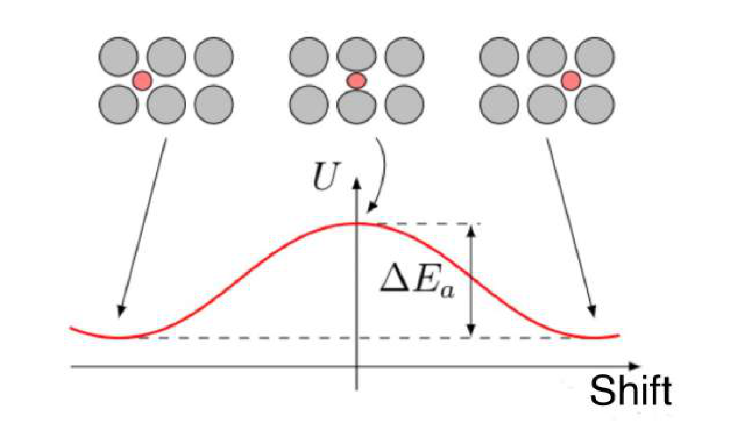
A qualitative diffusion scheme in a solid and the meaning of energy ΔEa.
B1 Using the program B1.py find by hand the value Φ and the thickness d of SiO2 film. The program B1.py reads values from a file B1.txt automatically and outputs an approximating graph Ψ,Δ from λ, for the values of the angle Φ entered by you in degrees and the thickness d of the dioxide film in nanometers. The input data is limited: 20∘≤Φ≤80∘, d≤250 nm.
B2 Using the program B2.py find by hand the value Φ and the thickness d of SiO2 film. The program works similarly to the previous B1.
For a detailed study of the oxidation rate, you can get ellipsometric data from your colleague, measured from a real-time oxidizing silicon substrate. At the initial moment t=0, he puts pure silicon inside the furniture with a temperature T, and every 2 min mesures the spectrum Ψ,Δ from λ at a fixed angle Φ, which you tell him.
In the file B_in.txt you specify the name of the experiment, the angle Φ in degrees, the temperature T in degrees Celsius, and the duration of the experiment in minutes in the form of a table:
Name
Φ,∘
T,∘C
t,min
test
50
1000
40
⋮
⋮
⋮
⋮
The input data is limited as 20∘≤Φ≤80∘, 800∘C≤T≤1200∘C, t≤200 min. The name of the experiment should not contain spaces and tabs. The separator between the integer and fractional parts of a number is a dot. The separator between the columns is a tab. Next, you run the program gen_data.exe which simulates your colleague conducting an experiment in accelerated mode. You can interrupt the execution of this program at any time, and the results of the measurements already performed will be saved on your computer. You can automatically process the measurement data using the program B.py which uses the same file B_in.txt . This program uses the results of the work gen_data.exe, selects the value of d for each point and calculates the statistical error of this value. Keep in mind that processing may take several minutes. The results of the program B.py are located in the /res folder in the form of tables and graphs d(t). An example of an automatically generated program B.py tables in the /res folder:
t,min
d,nm
Δd,nm
2
17.3
0.3
⋮
⋮
⋮
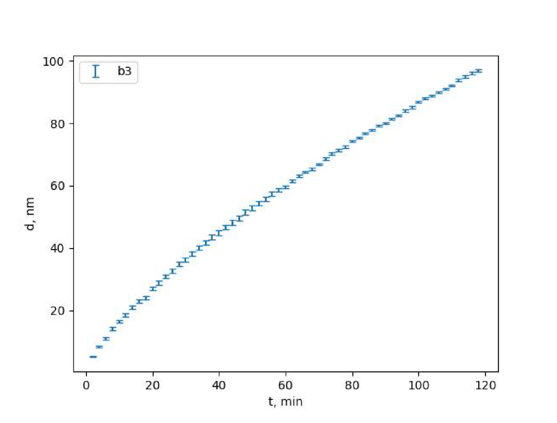
B3 Get the data for the dependence of the film thickness d of silicon dioxide on the time t during oxidation at a temperature of t=1000∘C for 120 min. Attach the graph obtained by the program B.py to the report.
Now let us consider the theoretical aspects of thermal oxidation. According to the Deal-Grove model, three processes are responsible for the rate of increase in the thickness of the silicon oxide layer:
diffusion of oxygen to the surface SiO2;
diffusion of oxygen through the layer SiO2;
oxidation reaction Si+O2→SiO2 at the interface SiO2/Si.
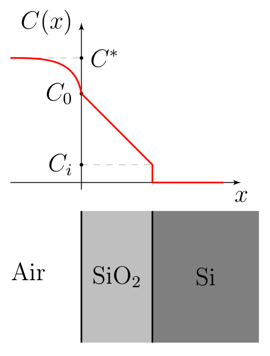
Thus, the concentration of oxygen C (dimension mol/m3) changes as it moves deeper into the sample. In the air, far away from the substrate, the oxygen concentration is C∗; inside the silicon dioxide layer, the concentration decreases linearly from C0 to Ci; inside silicon, the oxygen concentration is zero.
Let us consider a model for describing these processes. Specific (i.e. per unit surface area) the flow rates of each of the three processes F1, F2, F3 (units of measurement — mole/(c⋅m2)) we define as follows:
The diffusion rate is F1=h(C∗−C0), where h is a certain coefficient characterizing diffusion in the gas phase.
Counting the diffusion rate F2=dD(C0−Ci), where D is the diffusion coefficient of oxygen in the dioxide, depending on the temperature T, and d is the thickness of the silicon dioxide film.
The rate of the oxidation reaction F3=kCi, where k is the constant of the rate of the oxidation reaction, depending on the temperature T.
B4 Express the growing velocity v of film thickness change in terms of the oxidation reaction rate F3, the molar mass μSiO2 and the density ρSiO2 of silicon dioxide. Assume that the air-dioxide boundary does not move.
B5 Assuming the problem to be quasi-stationary (the establishment times of all processes are much less than the film rise time), express C0 and Ci in terms of C∗, the velocity constants h, k, D and the film thickness d.
B6 Get the differential equation for the thickness d of the dioxide film and get its solution with the initial condition d(t0)=d0 in the form
d2+Ad=B(t+τ),
where τ contains information about the initial conditions, and the constants A and B are related to the kinetics of oxidation. Express A and B in terms of h, k, D, C∗, μSiO2 and ρSiO2.
Experiments show that blowing with air (changing the profile C(x) above the surface), doesn’t change the rate of the process. Therefore we will consider h≫k.
At the beginning of the oxidation process, the stationary model is not applicable, so it is used starting from the minimum thickness d0=25 nm. Enter into the program B7.py the data from the file B_in.txt and get the parameters B and B/A automatically. If the maximum film thickness obtained in the experiment is less than d0, then the program B7.py outputs ”Final layer is too thin to approximate”.
If the program returns the error ”FileNotFoundError”, run the files gen_data.exe and B.py sequentially with the input data you need, previously entered in the B_in.txt.
B7 Get the values of the parameters B and B/A for five different temperatures T. Save the results into a file B8_in.txt in the form of a table.
T,∘C
B,nm2/min
ΔB,nm2/min
B/A,nm/min
Δ(B/A),nm/min
1000
174
4
1.21
0.02
⋮
⋮
⋮
⋮
⋮
The dependence of the reaction rate constant k on temperature T is associated with the energy ΔEb of breaking the bond Si−Si in a silicon crystal, and then the relation between them:
k∝e−ΔEb/kBT.
The diffusion coefficient in solids is also related to temperature via the so-called activation energy ΔEa, and the quantitative dependence has the form:
D∝e−ΔEa/kBT
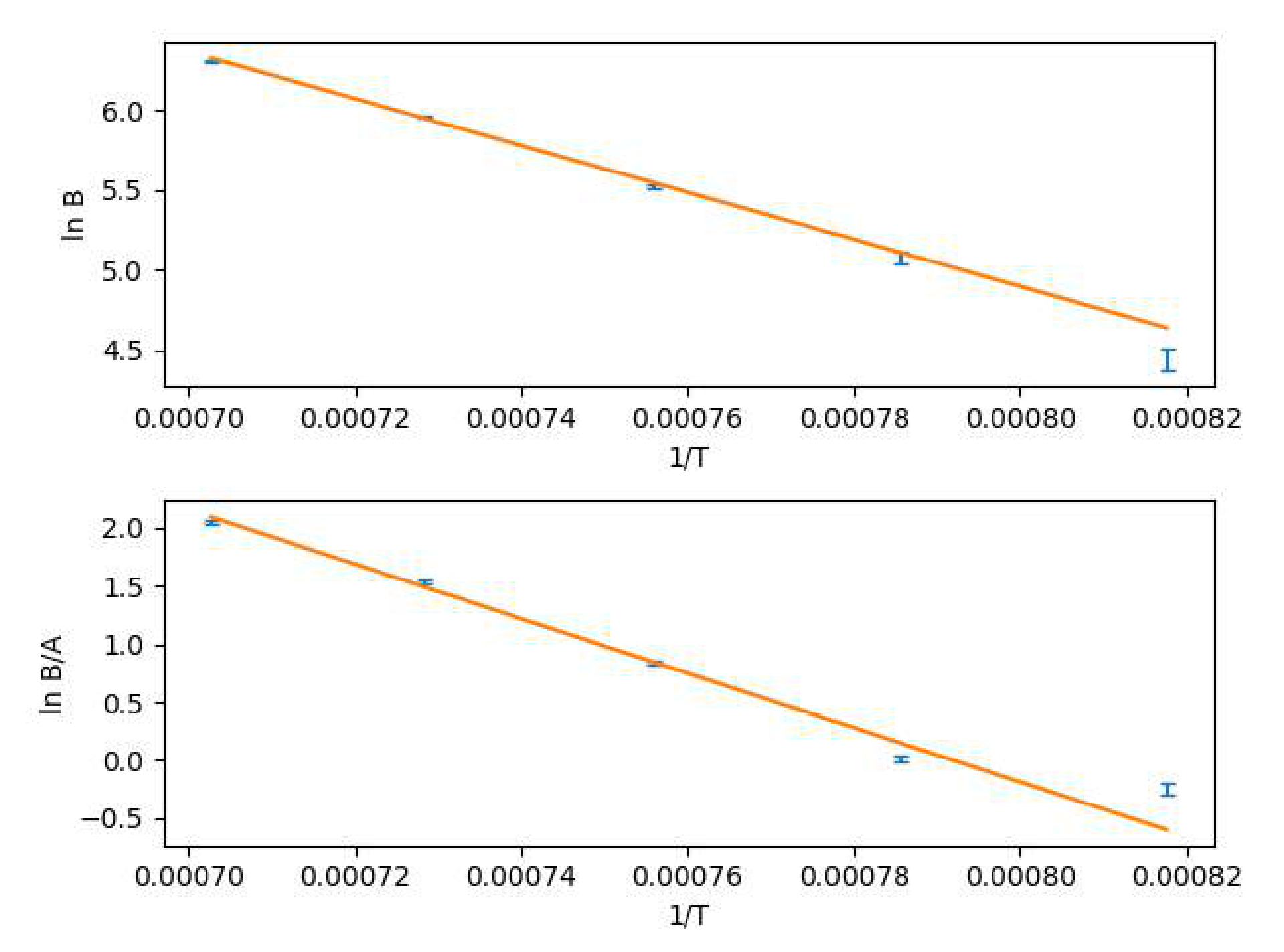
Using the program B8.py you can plot graphs ln(B⋅min/nm2) from 1/T and ln(B/A⋅min/nm)from 1/T and determine the parameters of the automatically drawn lines.
Boltzmann constant kB=1.38⋅10−23 J/C, elementary charge e=1.60⋅10−19 C.
B8 Determine the values of ΔEb and ΔEa in electron volts. Attach the linearized graphs to the report.
Отговори
Part A. Theoretical principles of ellipsometry, A2k1x=cε1ωcosθ1,k2x=cωε2−ε1sin2θ1,k3x=cωε3−ε1sin2θ1
Part A. Theoretical principles of ellipsometry, A4A=k2x−k3xk2x+k3x,B=k1x−k2xk1x+k2x
Part A. Theoretical principles of ellipsometry, A6A=κ2x−κ3xκ2x+κ3x,B=κ1x−κ2xκ1x+κ2x,κix=εikix
Part A. Theoretical principles of ellipsometry, A7 77 °
Part B. Kinetics of oxidation, B1 Φ = 71.1°, d = 66.7 nm
Part B. Kinetics of oxidation, B2 Φ = 57°, d = 232 nm
Part B. Kinetics of oxidation, B4v=F3ρSiO2μSiO2
Part B. Kinetics of oxidation, B5C0=C∗1+hk+Dkd1+Dkd,Ci=C∗1+hk+Dkd1
Part B. Kinetics of oxidation, B6A=2D(k1+h1),B=2DC∗ρSiO2μSiO2
Part B. Kinetics of oxidation, B8 ΔEa = (1.38 ± 0.05) eV, ΔEb = (2.02 ± 0.14) eV
Решение
Part A. Theoretical principles of ellipsometry
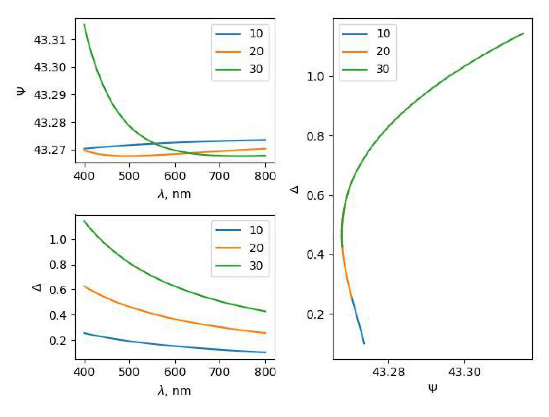
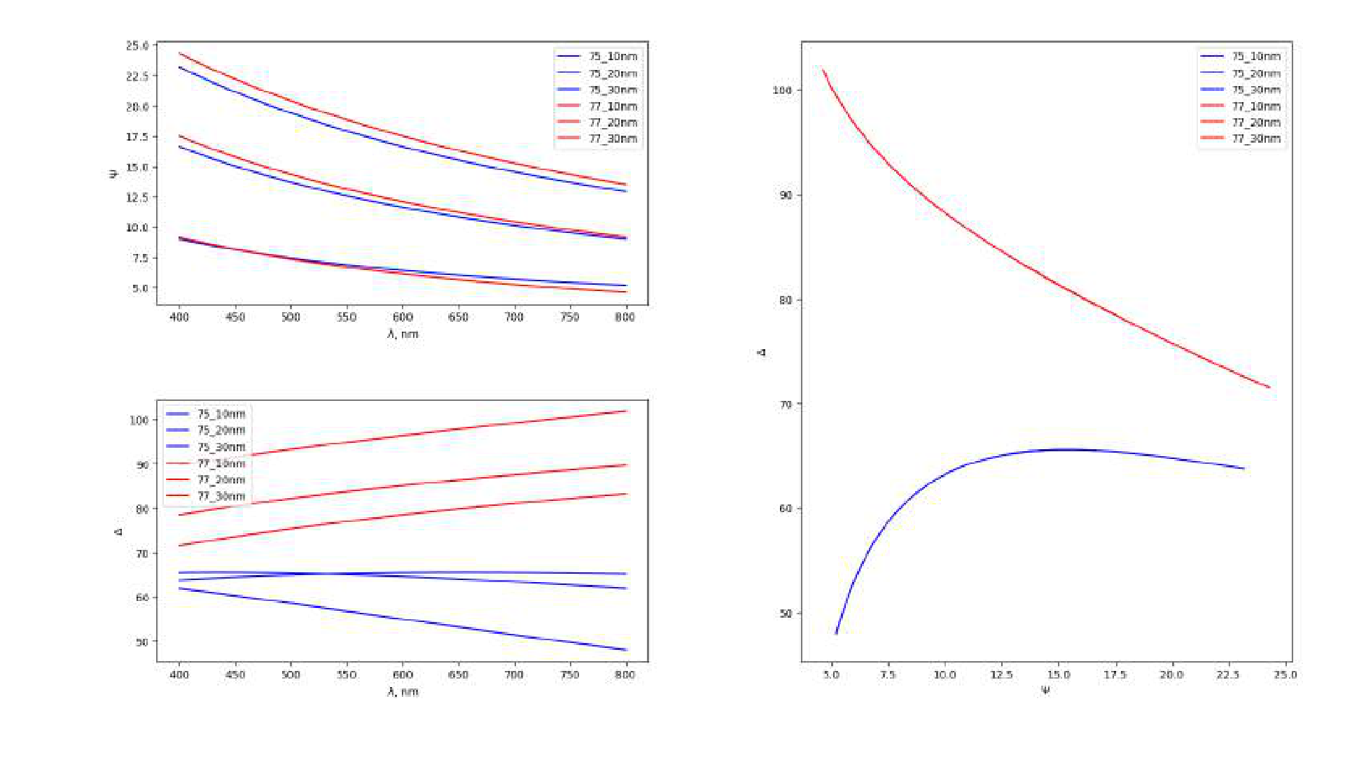
Dependencies for the angle of incidence of 20∘ and film thicknesses of 10 nm, 20 nm and 30 nm.A comparison of the dependencies for the angles of incidence of 75∘ and 77∘ and the film thickness of 10 nm, 20 nm and 30 nm.A comparison of the dependencies for the angles of incidence of 77∘ and 79∘ and the film thickness of 10 nm, 20 nm and 30 nm.
A1 A given system of equations for scalar complex amplitudes must be performed at any point of the interface between media:
we get the expression reduced to the required form.
A5 Similarly, A3 records the conditions at the two interfaces, taking into account the connection of electric and magnetic fields in the EM wave: εε0μ0E=B:
A7 We will receive graphs for three thicknesses: 10, 20 and 30 nm. At low angles of incidence, it can be seen that the maximum range of Ψ is hundredths degrees, while θ∼70∘, the maximum range of Φ is tens of degrees . The maximum sufficiency is reached when
θopt=77∘.
The corresponding graphs for comparison are given below.
θopt=77∘
Part B. Kinetics of oxidation
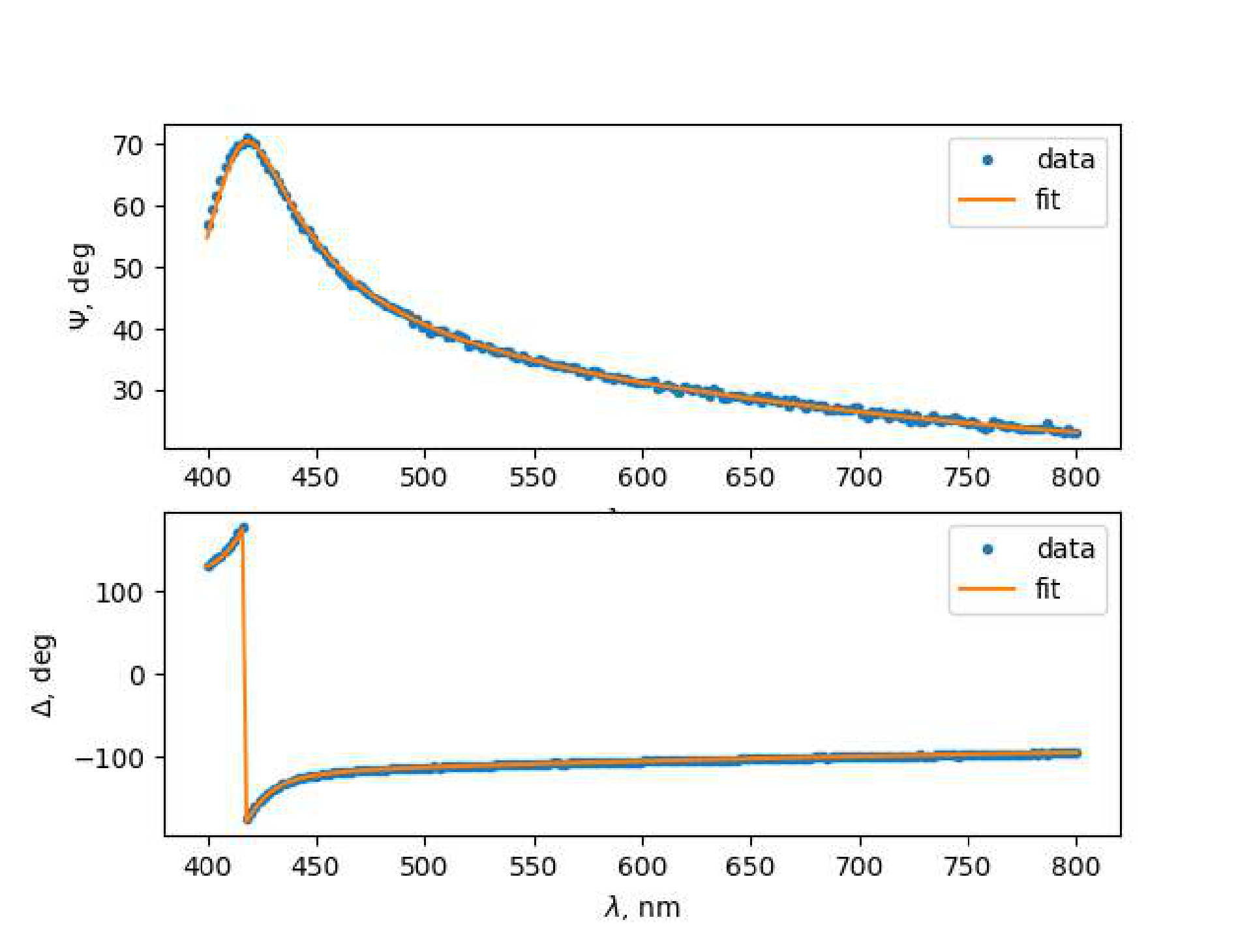
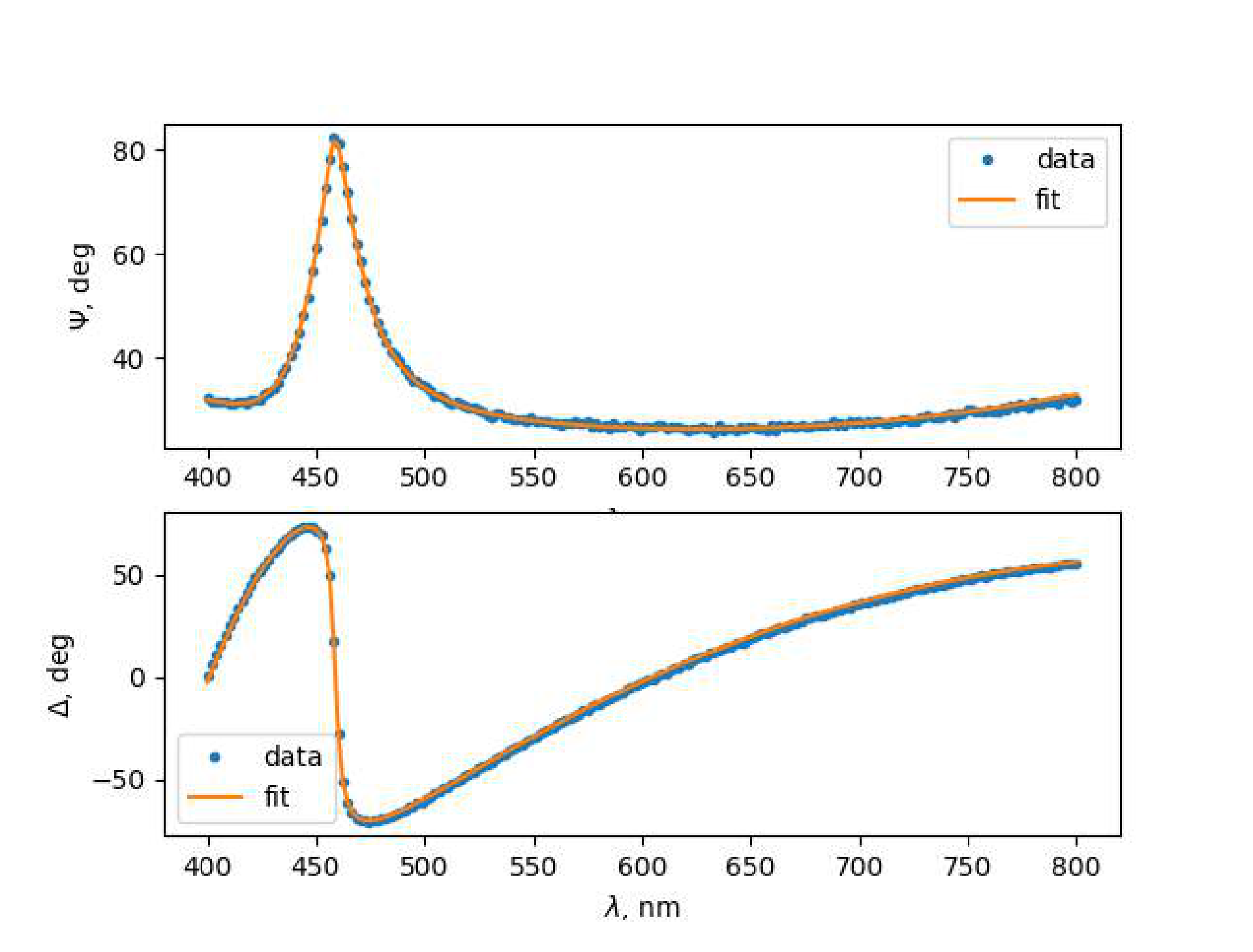
The graph for Φ=71∘,d=67nm.The graph for Φ=57∘,d=232nm.
B1 Let us describe the search algorithm for optimal Φ and d. First enter arbitrary Φ and d in B1.py. Next, on each step we try to change Φ or d a bit, and look at the "error" given out by the program B1.py. If the error decreases, we continue to change Φ or d in the same direction (e.g. if we have lowered Φ by 1∘, and the error have decreased, then on the next step we also lower Φ by 1∘). Finally, we will reach such Φ and d that any small changes of them lead to the increasing of the error, i.e. we reach the minimal possible error. It means that we have found optimal Φ and d.
One can see on the graph how fitting data correspond to the colleague’s ones, but the numerical parameter of the approximation quality is the error giving by the program B1.py.
Φ=71.1∘d=66.7nm
B2 The search algorithm for optimal Φ and d coincides with the such one in part B1.
Φ=57∘d=232nm
B3 Set name = b3, Phi = 77, T=1000, tmax=120 in B_in.txt, then run gen_data.exe and B.py consistently. In "res" folder we get the file with desired graph. Note that we substitute Φ=θopt from A7 in order to increase the quality of the experiment.
B4 Consider a small time period Δt and a part of SiO2-Si border having the area S. Then the mass of the Si oxided during Δt equals Δm=F3ΔtSμSiO2. On the other hand, the SiO2-Si border will move by vΔt, so the mass of SiO2 appeared equals Δm=ρSiO2SvΔt. Thus ρSiO2vSΔt=F3ΔtSμSiO2, so ρSiO2v=F3μSiO2.
v=F3ρSiO2μSiO2
B5 Stationarity conditions gives F1=F2=F3, i.e. h(C∗−C0)=dD(C0−Ci)=kCi. From the second equality we get C0=(1+Dkd)Ci. Substitute it in h(C∗−C0)=kCi and get h(C∗−(1+Dkd)Ci)=kCi, what implies C∗=(hk+Dkd+1)Ci, so
B6 From B4 we have v=d˙=ρSiO2F3μSiO2=ρSiO2kCiμSiO2. Taking into account the expression for Ci obtained in B5 we get
d˙=C∗ρSiO2μSiO2k1+h1+Dd1
or, equivalently,
Dd˙⋅d+d˙⋅(k1+h1)−C∗ρSiO2μSiO2=0
Note that the left hand side equals
dtd(2Dd2+d⋅(k1+h1)−t⋅C∗ρSiO2μSiO2)=0
So
2Dd2+d⋅(k1+h1)−t⋅C∗ρSiO2μSiO2=const
where const can be found from the initial condition d(t0)=d0. Namely,
const=2Dd02+d0⋅(k1+h1)−t0⋅C∗ρSiO2μSiO2
So we get
d2+2D⋅(k1+h1)⋅d=2DC∗ρSiO2μSiO2(t+τ)
where τ=2DC∗μSiO2const⋅ρSiO2.
A=2D(k1+h1),B=2DC∗ρSiO2μSiO2
B7 First create data necessary for B7.py. Set T, Φ=θopt=77∘, tmax=120 in B_in.txt, then run gen_data.exe and B.py, and finally, run B7.py five times, on each time entering name, T and Φ from B_in.txt. We write every output of B7.py in the file B8_in.txt and get the table below.
Note that even for T=850∘C we get an error "Final layer is too thin to approximate", and for T=900∘C we get too high error rate, so it is reasonable to start with T=950∘C with a step 50∘C.
T,∘C
B,nm2/min
ΔB,nm2/min
B/A,nm/min
Δ(B/A),nm/min
950
85
6
0.780
0.044
1000
160
6
1.017
0.027
1050
251
4
2.310
0.044
1100
389
2
4.636
0.070
1150
551
4
7.751
0.188
B8 First plot the graphs lnB(T1) and lnAB(T1) using the program B8.py. In the console one can see the slopes of proposed linear approximations. Namely, the slope coefficient of lnB(T1) equals −(14671±625)∘C, and the slope coefficient of lnAB(T1) equals −(23418±1730)∘C (where K means one kelvin).
We get from B6 that
B=2DC∗ρSiO2μSiO2∝e−kBTΔEa
Thus the slope coefficient of the graph lnB(T1) equals −kBΔEa. So ΔEa=(2.208±0.086)⋅10−19 J, or, equivalently,