ISPhO 2026, Теория — Задача 3. PN junctions in semiconductors
ISPhO Theory Q3-1 — PN junctions in semiconductors · 10 т.
Бележка
You may use the following physical constants: – electric constant; – absolute value of electron charge; – Boltzmann constant. For the silicon based diode, considered in this problem: – dielectric constant; – temperature; ; ; – concentration of electrons and holes in semiconductor without impurities.
Условие
Semiconductors are materials with electric conductivity significantly lower than conductivity of metals. Unlike insulators, conductivity of semiconductors is not zero and rapidly increases with temperature. This fact can be explained by the increase of charge carrier concentration due to thermal excitations.
There are two types of charge carriers in semiconductors, electrons and holes. Holes are positively charged particles, that appear in place where an electron is absent. Hole charge is equal to absolute value of electron charge. In a pure semiconductor concentrations of electrons and holes are equal to each other.
Semiconductor devices, in particular diodes and transistors, are widely used in modern electronics. In this problem we consider one of the simplest models of a semiconductor diode.
Charge carriers concentration in semiconductors can be easily modified by adding a small amount of impurities, i.e., atoms of another chemical element. Impurities that increase the electron concentration are referred to as donors, semiconductor with excess of donors is called -type (from negative) semiconductor. Hole concentration in -type semiconductor is much lower than electron concentration. Impurities that increase holes concentration are referred to as acceptors, semiconductor with excess of acceptors is called -type (from positive) semiconductor.
Consider a contact of two semiconductors of and types ( junction). In practice we can dope different parts of semiconductor with different types of impurities. The current through the junction depends on the polarity of applied voltage. The resulting structure is a semiconductor diode.
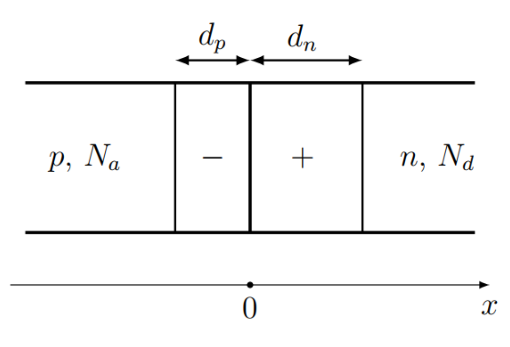
In this problem we consider the following model of a diode (Fig. 1).
- All physical quantities depend only on one coordinate .
- The region is a -type semiconductor with impurity concentration .
- The region is a -type semiconductor with impurity concentration .
- Near the junction electrons and holes diffuse through the boundary. As a result, in region there is a negatively charged layer of width , and in region there is a positively charged layer of width . These layers are called depletion layers.
- In depletion layers the main charge carrier concentration (holes in -type semiconductors and electrons in -type semiconductor) is almost zero, outside of the layers their concentration is constant and equal to the concentration of impurities.
- Volume charge density in depletion layer can be calculated from assumption that each donor impurity has charge , and each acceptor impurity has charge , where – absolute value of electron charge.
You may use the following physical constants:
- – electric constant;
- – absolute value of electron charge;
- – Boltzmann constant.
For the silicon based diode, considered in this problem:
- – dielectric constant;
- – temperature;
- ;
- ;
- – concentration of electrons and holes in semiconductor without impurities.
Part A. Electrostatics (5.0 points)
In this part we consider electric field distribution in the junction without external voltage. From symmetry considerations, the electric field is parallel to the axis, the only non-zero component is .
Part B. Junction with external voltage (5.0 points)
Now we apply voltage to the junction (Fig. 2). The voltage is positive if applied to the -type semiconductor. The applied voltage changes energies of electrons and holes in the -type semiconductor, while energies in -type semiconductor are the same. Assume that electrons and holes concentrations and obey the Boltzmann distribution:
where , are potential energies of an electron or a hole in corresponding point, – absolute temperature, , – normalization constants, determined by the concentration of impurities and correspondingly. Concentration ratio of electrons and holes to the right and to the left of the junction is determined by energy difference:
If applied voltage , holes move from -type semiconductor to -type, while electrons move from -type semiconductor to -type. In addition, concentration of electrons in -type semiconductor is determined by impurity concentration and does not change, while hole concentration increases. Similarly in -type semiconductor hole concentration does not change while electron concentration increases.
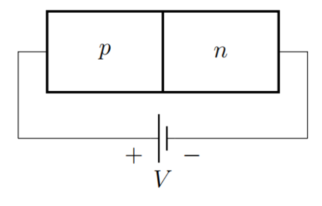
We obtained, that after the voltage is applied, the hole concentration in -type semiconductor and electron concentration in -type semiconductor are different from equilibrium ones. Electrons can move to the vacant places, corresponding to holes. In such process the electron and the hole disappear (recombine). Boltzmann distribution does not take recombination into account. Therefore without diffusion charge carries concentrations change to equilibrium values.
To be specific, consider holes in -type semiconductor outside of depletion layer. Denote the hole concentration by , equilibrium concentration without diffusion by . The rate of concentration change due to recombination can be expressed as
where is time of hole recombination. Holes flux (number of holes that transfer through the unit area in unit time) due to diffusion is described by the formula
where is holes diffusion coefficient.
The characteristic length, over which the hole concentration changes due to recombination, is much larger than the depletion layer width. Therefore we can neglect recombination in depletion layer. The current through the junction can be calculated as a sum of electron current and hole current, independent of each other. To calculate the hole current we can consider -type semiconductor near the depletion layer boundary, where the current is determined by diffusion and hole concentration can be calculated from Boltzmann distribution. The electron current can be found in the same way.
The expression for the electron current can be obtained by analogy, if we replace hole concentration by electron concentration , diffusion coefficient, recombination time and characteristic length by corresponding values for electrons, , and . Equilibrium holes and electrons concentrations are given by
where is concentration of electrons or holes in semiconductor without impurities.
The numerical values of the parameters are:
- ;
- , ;
- .
A.1 Total electric charge near the junction must be equal to zero. Using this fact, write an equation connecting widths of depletion layers , and impurities concentrations , . [0,5 т.]
A.2 Show that the following equation holds for electric field
where – volume charge density in the corresponding point. [0,5 т.]
A.3 Find the electric field as a function of . Assume that far from junction the field is equal to . Express the answer in terms of , , , , , and . [1 т.]
A.4 Find the electrostatic potential as a function of . Assume that . Express the answer in terms of , , , , , and . Determine the potential difference at large distance to the junction . [1 т.]
A.5 Draw a qualitative plot of the potential as function of . [0,5 т.]
A.6 Actually, the potential difference is determined by the material properties and the temperature. Knowing the potential difference, one can calculate depletion layers widths. Express the widths , in terms of , , , , and . Calculate their numerical values for . [1 т.]
A.7 Determine the maximum value of the electric field in the junction . Express the answer in terms of , , , , and . Calculate its numerical value for . [0,5 т.]
B.1 Let denote the concentration of electrons in -type semiconductor without external voltage. Similarly let denote the concentration of holes in -type semiconductor without external voltage. Determine electron concentration in -type semiconductor and hole concentration in -type semiconductor after the voltage is applied. Consider region outside of depletion layers, where electric field is zero. Express the answers in terms of , , , , and . [0,5 т.]
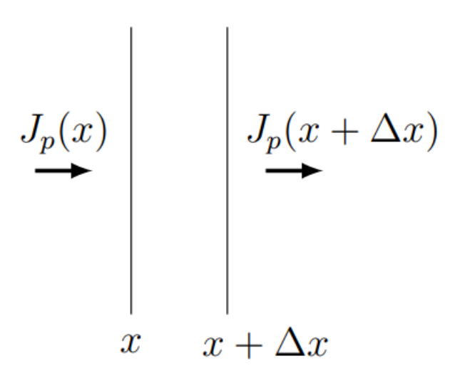
B.2 Consider the volume between the planes with coordinates and (Fig. 3). Write down the condition that the holes concentration in this volume does not change. Take into account the holes flux through the two planes and holes recombination. In the limit obtain a differential equation for the concentration deviation from equilibrium value as a function of . The answer may also include and . [1 т.]
B.3 Find the distance , over which the deviation of holes concentration from equilibrium decreases by times. Express the answer in terms of , . Compute numerical value for , . [0,6 т.]
B.4 Determine the hole concentration in region as a function of coordinate (in -type semiconductor outside of the depletion layer). Express the answer in terms of , , , , , and . [0,8 т.]
B.5 Determine the density of hole diffusion current at the boundary of depletion layer . Express the answer in terms of , , , , , and . [0,8 т.]
B.6 The junction cross section area is . Derive the expression for the total current through the junction as a function of applied voltage , semiconductor parameters , , , , , , and constants , . [0,8 т.]
B.7 Draw a qualitative plot of the relation , obtained in previous task. [0,3 т.]
B.8 Calculate the numerical values of the saturation current at large negative voltage, and the value of current for . [0,2 т.]
Решение
Внимание: Непълно решение
В архива няма официално решение на тази задача.
Оригинал в Архива: T3.pdf