IPhO 1975, Теория и експеримент — Задача 4. Semiconductor element
Problems of the 8th International Physics Olympiad (Güstrow, 1975) · 7 юли 1975 г. · 20 т.
Увод
Gunnar Friege & Gunter Lind
Introduction
The 8th International Physics Olympiad took place from the 7.7. to the 12.7. 1975 in Güstrow, in the German Democratic Republic (GDR). Altogether, 9 countries with 45 pupils participated. The teams came from Bulgaria, the German Democratic Republic, the Federal Republic of Germany (FRG), France, Poland, Rumania, Tchechoslowakia, Hungary and the USSR. The entire event took place in the pedagogic academy of Güstrow. Pupils and leaders were accommodated inside the university academy complex. On the schedule there was the competition and receptions as well as excursions to Schwerin, Rostock, and Berlin were offered. The delegation of the FRG reported of a very good organisation of the olympiad.
The problems and solutions of the 8th International Physics Olympiad were created by a commission of university physics professors and lecturers. The same commission set marking schemes and conducted the correction of the tests. The correction was carried out very quickly and was considered as righteous and, in cases of doubt, as very generous.
The main competition consisted of a 5 hour test in theory and a 4.5 hour experimental test. The time for the theoretical part was rather short and for the experimental part rather long. The problems originated from central areas of classical physics. The theoretical problems were relatively difficult, although solvable with good physics knowledge taught at school. The level of difficulty of the experimental problem was adequate. There were no additional devices necessary for the solution of the problems. Only basic formula knowledge was requested, and could be demanded from all pupils. Critics were only uttered concerning the second theoretical problem (thick lens). This problem requested relatively little physical understanding, but tested the mathematical skills and the routine in approaching problems (e.g. correct distinction of cases). However, it is also difficult to find substantial physics problems in the area of geometrical optics.
Altogether 50 points were the maximum to achieve; 30 in the theoretical test and 20 in the experimental test. The best contestant came from the USSR and had 43 points. The first prize (gold medal) was awarded with 39 points, the second prize (silver medal) with 34 points, the third prize (bronze medal) with 28 points and the fourth prize (honourable mention) with 22 points. Among the 45 contestants, 7 I. prizes, 9 II. prizes, 12 III. prizes and 8 IV. prizes were awarded, meaning that 80 % of all contestants were awarded.
The following problem descriptions and solution are based mainly on a translation of the original German version from 1975. Because the original drafts are not well preserved, some new sketches were drawn. We also gave the problems headlines and the solutions are in more detail.
Remark: This article was written due to the special request to us by Dr. W. Gorzkowski, in order to close one of the last few gaps in the IPhO-report collection.
Contact: Dr. Gunnar Friege, Leibniz-Institute for Science Education (IPN) at the University of Kiel, Olshausenstr. 62, 24098 Kiel, Germany, friege@ipn.uni-kiel.de
Условие
Experimental problem: “Semiconductor element”
In this experiment a semiconductor element 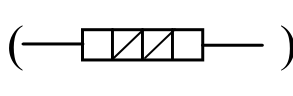 , an adjustable resistor (up to 140 Ω), a fixed resistor (300 Ω), a 9-V-direct voltage source, cables and two multimeters are at disposal. It is not allowed to use the multimeters as ohmmeters.
a) Determine the current-voltage-characteristics of the semiconductor element taking into account the fact that the maximum load permitted is 250 mW. Write down your data in tabular form and plot your data. Before your measurements consider how an overload of the semiconductor element can surely be avoided and note down your thoughts. Sketch the circuit diagram of the chosen setup and discuss the systematic errors of the circuit. [6 т.]
b) Calculate the resistance (dynamic resistance) of the semiconductor element for a current of 25 mA. [3 т.]
c) Determine the dependence of output voltage from the input voltage by using the circuit described below. Write down your data in tabular form and plot your data.
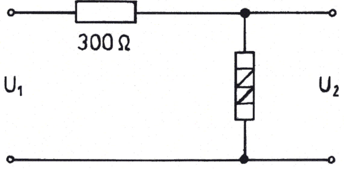
The input voltage varies between 0 V and 9 V. The semiconductor element is to be placed in the circuit in such a manner, that is as high as possible. Describe the entire circuit diagram in the protocol and discuss the results of the measurements. [5 т.]
d) How does the output voltage change, when the input voltage is raised from 7 V to 9 V? Explain qualitatively the ratio . [3 т.]
e) What type of semiconductor element is used in the experiment? What is a practical application of the circuit shown above? [3 т.]
Hints: The multimeters can be used as voltmeter or as ammeter. The precision class of these instruments is 2.5% and they have the following features:
| measuring range | 50 µA | 300 µA | 3 mA | 30 mA | 300 mA | 0,3 V | 1 V | 3 V | 10 V |
|---|---|---|---|---|---|---|---|---|---|
| internal resistance | 2 kΩ | 1 kΩ | 100 Ω | 10 Ω | 1 Ω | 6 kΩ | 20 kΩ | 60 kΩ | 200 kΩ |
Отговори
b) About 10 Ω ± 50% in the backward direction and about 1 Ω ± 50% in the flux direction.
d) 0.1 V
The official solution gives ΔU2 = 0.1 V ± 50%.
e) A Z-diode (Zener diode); also correct: diode and rectifier. The circuit can be used for stabilisation of voltages.
Решение
Solution of the experimental problem:
a) Some considerations: the product of the voltage across the semiconductor element and current through this element is not allowed to be larger than the maximum permitted load of 250 mW. Therefore the measurements have to be processed in a way, that the product is always smaller than 250 mW.
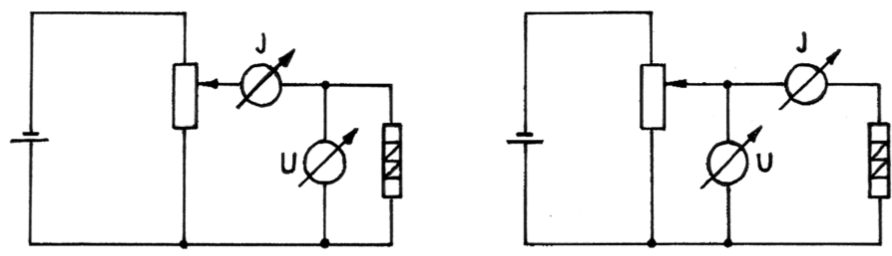
The figure shows two different circuit diagram that can be used in this experiment:
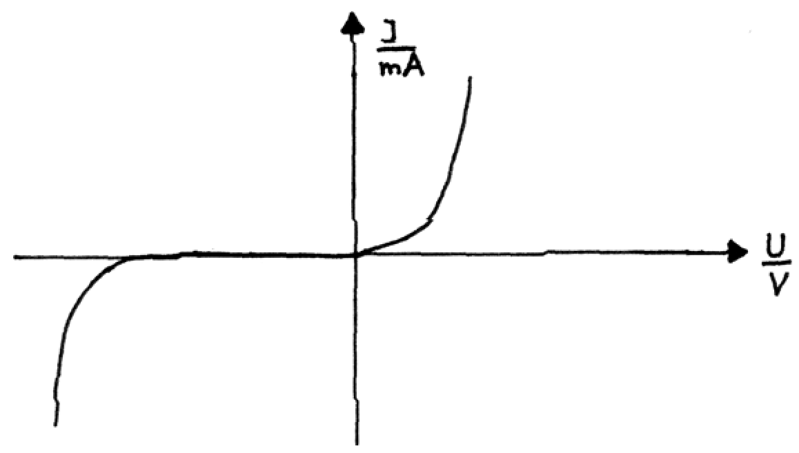
The complete current-voltage-characteristics look like this:
The systematic error is produced by the measuring instruments. Concerning the circuit diagram on the left (“Stromfehlerschaltung”), the ammeter also measures the current running through the voltmeter. The current must therefore be corrected. Concerning the circuit diagram on the right (“Spannungsfehlerschaltung”) the voltmeter also measures the voltage across the ammeter. This error must also be corrected. To this end, the given internal resistances of the measuring instruments can be used. Another systematic error is produced by the uncontrolled temperature increase of the semiconductor element, whereby the electric conductivity rises.
b) The dynamic resistance is obtained as ratio of small differences by
The dynamic resistance is different for the two directions of the current. The order of magnitude in one direction (backward direction) is 10 Ω ± 50% and the order of magnitude in the other direction (flux direction) is 1 Ω ± 50%.
c) The complete circuit diagram contains a potentiometer and two voltmeters.
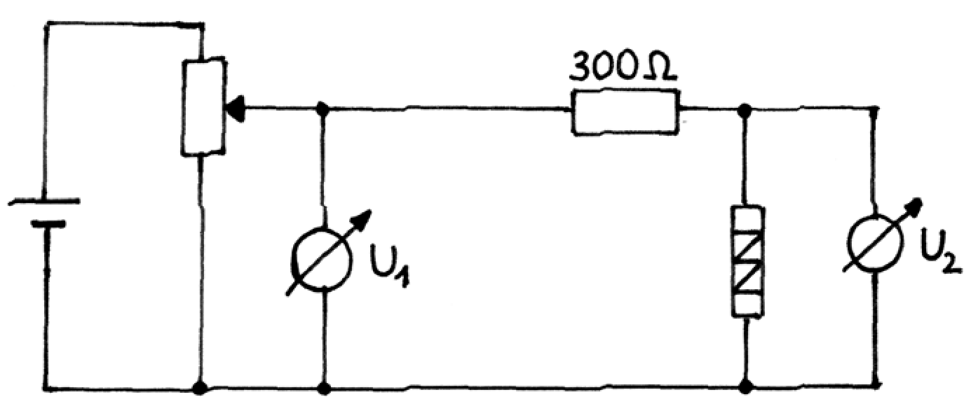
The graph of the function has generally the same form for both directions of the current, but the absolute values are different. By requesting that the semiconductor element has to be placed in such a way, that the output voltage is as high as possible, a backward direction should be used.
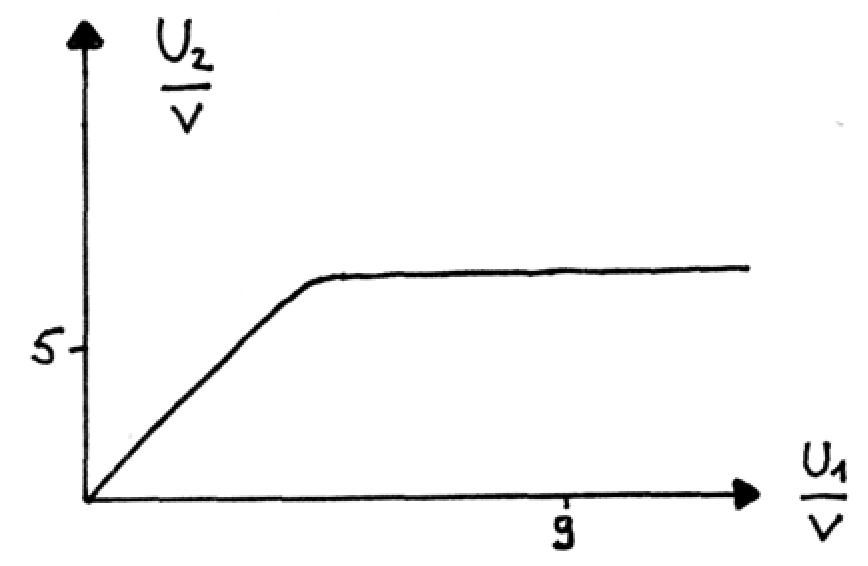
Comment: After exceeding a specific input voltage the output voltage increases only a little, because with the alteration of the current increases (breakdown of the diode) and therefore also the voltage drop at the resistance.
d) The output voltages belonging to and are measured and their difference is calculated:
Comment: The circuit is a voltage divider circuit. Its special behaviour results from the different resistances. The resistance of the semiconductor element is much smaller than the resistance. It changes nonlinear with the voltage across the element. From follows in the case of .
e) The semiconductor element is a Z-diode (Zener diode); also correct: diode and rectifier. The circuit diagram can be used for stabilisation of voltages.
Marking scheme
Experimental problem: “Semiconductor element” (20 points)
| Part a – considerations concerning overload, | 6 points |
|---|---|
| circuit diagram, | |
| experiment and measurements, | |
| complete current-voltage- | |
| -characteristics | |
| discussion of the systematic errors | |
| Part b – equation (1) | 3 points |
| dynamic resistance for both directions | |
| correct results within ±50% | |
| Part c – complete circuit diagram, | 5 points |
| measurements, | |
| graph of the function , | |
| correct comment | |
| Part d – correct within ±50%, | 3 points |
| correct comment | |
| Part e – Zener-diode (diode, rectifier) and | 3 points |
| stabilisation of voltages |
Remarks: If the diode is destroyed two points are deducted.
If a multimeter is destroyed five points are deducted.
Оригинал в Архива: ipho75.pdf